![]()
HomePRODUCTSBuried-blind via PCB
0755-23087429
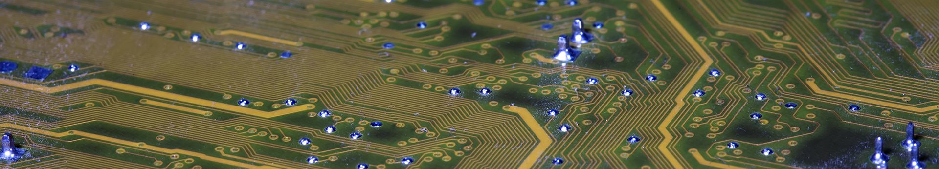
Buried-blind via PCB
PRODUCT
Layer count:8
Board thickness:1.2mm
Base materials:FR4 S1000-2
Finished size:205*145mm
Surface finish:沉金+OSP
Line width/line space:3/3mil
Minimum hole:0.10mm
Solder resist color:Sensitive green
Cu thickness:inner layer H OZ outer layer 1 OZ
1, the structure is complex, the two order HDI:
Blind hole L1-L2, L7-L8
Buried hole L2-L3, L3-L6, L6-L7
Through hole L1-L8
2, multiple pressure and copper;
3, the need for laser drilling blind hole;
4, the line spacing is small, etching difficult;
5, pressure, line, high precision drilling requirements;
6, multiple thin copper surface.
